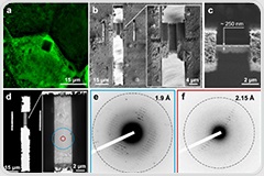
Discover how fluorescence-guided cryo-FIB milling enables reliable localization of intracellular protein crystals within vitrified cells, eliminates purification steps, and supports precise, site-specific lamella preparation for subsequent TEM electron diffraction analysis.
Advancements in multiplex imaging are reshaping cancer diagnostics, leveraging spatial biology and AI for improved biomarker discovery and treatment strategies.
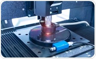
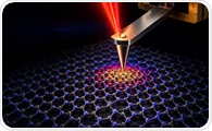
Researchers introduced TFM-IR, an ambient-condition infrared microscopy method that uses torsional cantilever dynamics and nonlinear frequency mixing to map in-plane and out-of-plane photothermal responses at the nanoscale. The technique resolved anisotropic strain in mica nanobubbles and achieved near-nanometer optical imaging in twisted bilayer graphene, enabling site-resolved spectroscopy within individual moiré cells.
How would you rate today's newsletter?
Stay updated with the latest in health and medical news! Follow News‑Medical.net on Google News for real‑time updates. Click here to follow us now.
Why did you receive this email?
You are receiving this email because you subscribed to updates from AZoNetwork UK Ltd. on one of
our websites
and requested to be notified of additional information.