Microscopes are of three basic types: optical, electron (or ion), and scanning probe.
The modern optical or light microscope was developed in the mid-19th century. Optical microscopes use transparent lenses and visible light to enable viewing of objects in the micrometer scale, e.g., red blood cells, human hair. However, limitations of light microscopy such as its low resolution were an encouragement for the invention of the electron microscope in 1931.
Electron microscopes use electromagnetic or electrostatic lenses and a beam of charged particles (instead of light) to view particles of size in the nanometer scale, e.g., atoms. They have the capability to magnify objects more than 500,000 times, thus allowing visualization of tiny structures such as DNA and microbes at very high resolution.
Scanning probe microscopy was developed in the 1980s to study atomic surfaces at nanoscale resolution. These microscopes don’t use lenses. Instead, they use a sharp needle as a probe to interact with the surface of the sample and map the interactions to form an image. This invention revolutionized nanotechnology and allowed study and manipulation of atoms to create different structures.
Optical microscopy
Optical microscopy (light microscopy) is a very common tool in biological research which employs visible light to magnify tiny objects. Light sources commonly used in optical microscopes include arc-discharge lamps, incandescent tungsten-halogen bulbs, LEDs, and lasers. Leica Microsystems, imaging equipment maker, offers automated light microscopes with choice of illumination between halogen and LED.
Various illumination techniques used in optical microscopes include bright field, dark field, cross-polarized light, and phase contrast illumination. These techniques provide increased contrast while viewing the sample. Analytical instruments manufacturer, Bruker offers specialized 3D optical microscopes that are ideal for precision 3D surface measurements in the automotive, LED, aerospace, semiconductor, solar, and medical device manufacturing industry.
Some techniques used to gather specific data give rise to other types of light microscopy including fluorescence, confocal, UV, near-infrared and multiple transmission microscopies. These are widely used in clinical and industrial applications. Light microscopes from Olympus, manufacturer of opto-digital products for the life science industry, are customizable with optical and digital imaging capabilities and are widely used in quality control and new product checking in the electronics, metals, and chemicals industries.

Electron microscopy
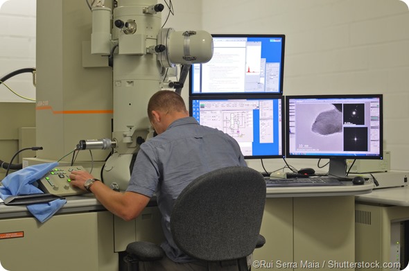
The electron microscope uses an electron beam to form an image of the sample. It has greater resolving power compared to the light microscope which allows the viewing of finer details of tiny objects. It uses electromagnetic or electrostatic lenses to control the path of electrons which are sensitive to magnetic fields. The resolving power of an electron microscope is inversely proportional to the irradiation wavelength.
The electron microscope is extensively used in scientific laboratories globally to study biological samples such as cells, microbes, and biopsies, crystalline or metal structures, and surface characteristics of various materials.
Scanning electron microscopes from Zeiss provide high detection efficiency and sub-nanometer resolution. Some of the company’s microscopes combine field emission Scanning Electron Microscopy (FE-SEM) technology and advanced analytics and can produce precise images of surfaces, particles, and nanostructures. The MultiSEM technology used in these products help achieve speeds of close to 91 parallel electron beams and they can image centimeter-scale samples at a nanometer resolution.
Scanning electron microscopes from FEI offer extremely high resolution and enhanced contrast at the sub-nanoscale. They are used in material topography inspections and offer better magnification than optical microscopes do.
Scanning probe microscopy
Scanning probe microscopes (SPMs) use a range of tools to produce images of surfaces and structures at the nanoscale level. A sharp physical probe scans the sample surface and sends the data gathered to a computer that generates a high resolution image of the sample surface, which can be visualized by the user.
Unlike with optical microscopes, SPM users don’t see the sample surface directly - they see an image that represents the surface of the sample. Different types of SPMs are atomic force microscopes, magnetic force microscopes, and scanning tunneling microscopes.
References
- https://www.jic.ac.uk/
- http://www.olympus-ims.com/en/microscope/terms/feature10/
- http://www.zeiss.com/microscopy/en_de/products/scanning-electron-microscopes.html
- http://www.leica-microsystems.com/products/em-sample-prep/
- http://teachers.stanford.edu/activities/SPMReference/SPMReference.pdf
- http://www.fei.com/introduction-to-electron-microscopy/types/
- https://www.bruker.com/products/surface-and-dimensional-analysis/3d-optical-microscopes.html
- http://www.ruf.rice.edu/~bioslabs/methods/microscopy/microscopy.html
Further Reading
Last Updated: Jul 19, 2023
 Label-free polarized light reveals subtle red blood cell deformations