Sponsored Content by EV GroupMay 26 2021
At present, micro-electro-mechanical systems (MEMS) devices can be found in virtually every technology of day-to-day life. One prominent example of consumer devices is smartphones that integrate numerous MEMS devices, like MEMS-based filters for wireless communication and gyroscopes and accelerometers for motion sensing.
MEMS also happens to be a crucial technology for the automotive sector, and they range from accelerometers in airbag release systems to tire pressure monitoring systems or pressure sensors in engine management.
Particularly, MEMS devices for industrial and automotive applications are required to meet the highest standards in terms of reliability and performance, placing significant demands on manufacturing technologies.
For a long time, EVG has been a top supplier of wafer processing equipment for the MEMS sector. At present, constant innovation, excellent process knowledge and a wide product portfolio in the fields of wafer bonding and lithography ensure that MEMS customers are supported in designing state-of-the-art solutions for their advanced devices.
Optical lithography
A majority of the MEMS devices contain 3D structures that have tiny delicate moving parts and high topography. Therefore, manufacturing processes need thick resist processing and conformal coating over topographies together with exceptional alignment and exposure capabilities.
Apart from regular UV lithography, nanoimprint lithography (NIL) also provides nanostructuring for emerging applications in MEMS. Maskless exposure (MLE™) technology also allows dynamic patterning of photoresist, such as the potential of individual die annotation — a significant aspect for crucial industrial and automotive MEMS applications.
.jpg)
Image Credit: EV Group
Advanced resist processing [(B) (C) (T)]
- Specialty resist processing
- Multilayer processing
- Spin and spray coating capabilities
- Stream, puddle, spray and ultrasonically assisted development
High accuracy mask alignment [(A) (B) (C) (T)]
- Bond alignment
- High depth-of-focus exposure
- New UV-LED technology
- Lithography for both etching and metallization
Digital manufacturing with maskless exposure technology (MLE™) [(D) (A) (B) (C) (T)]
- Mask-free digital infrastructure
- Agile and smart from rapid prototyping to large-scale manufacturing
- Individual patterns ranging from die annotation to multiple project wafers
- Dynamic photoresist patterning with less than 2 µm space/line resolution
Nanoimprint lithography (NIL) for maximum resolution [(N)]
- Volume-proven wafer-level imprinting technology
- Proprietary SmartNIL® technology
- Cutting-edge wafer-level-optics capabilities
- Novel processing for Bio-MEMS
MEMS devices
.jpg)
Image Credit: EV Group
Process results
Lithography
.jpg)
Image Credit: EV Group
Bonding
.jpg)
Image Credit: EV Group
Wafer bonding
A majority of the MEMS devices must be protected against the external environment or should operate only under a controlled vacuum or atmosphere. Today, high levels of incorporation with CMOS chips also need sophisticated wafer-level packaging solutions for MEMS devices.
A majority of the MEMS are also based on technical substrates, like SOI wafers. Therefore, wafer-level bonding procedures have a key role to play in the production of MEMS devices
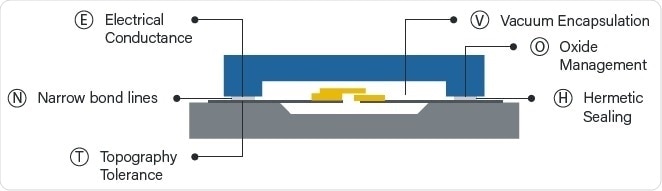
Image Credit: EV Group
Metal bonding for hermetic sealing and vacuum encapsulation (eutectic, solder, metal diffusion, and transient liquid phase (TLP)) [(E) (V) (H) (N)]
- Excellent mechanical strength
- Multipurpose interface properties
- High post-bond alignment precision
- Defined pressure encapsulation
Fusion bonding for engineered substrates [(V) (H)]
- Hybrid bonding
- MEMS-SOI substrates
- Heterogeneous integration for sophisticated semiconductor package
- Collective die transfer
Anodic bonding for consistent silicon-glass interfaces [(V) (H)]
- High post-bond temperature tolerance
- Optical transparency
- Highly strong and stable bond
- Triple-stack bonding (Si-glass-Si)
Topography tolerance with glass-frit bonding [(V) (T) (H)]
- Wide process window
- Intermediate glass layer
- Production has been proven for many years
- Planar electrical feed-throughs
Adhesive bonding for streamlined integration [(T) (H)]
- Ultra-thin adhesive layer transfer bonding
- Room-temperature bonding with UV-curing adhesives
- Temporary bonding/debonding
- Can be used with an array of substrate materials
High-end packaging with ComBond® technology [(O) (E) (V) (H) (N)]
- Vacuum encapsulation without getters
- High-vacuum handling and processing (<7E−8 mbar)
- Wafer surface activation
- Low-temperature Al-Al bonding
Process services and competence center
With advanced application cleanrooms and laboratories at its headquarters based in Austria, Japan and the United States, EVG is dedicated to delivering excellent process expterise to its global research and development and production partner and customer base.
Services span from feasibility studies and equipment demonstrations to small-to-medium-scale pilot-line production to reduce time to market.
In addition, EVG has established the Heterogeneous Integration Competence Center™, which has been developed to help clients leverage the company’s process expertise and solutions to allow new, improved applications and products that are driven by advancements in integration and packaging of systems.
.jpg)
Product range excerpt
Lithography
.jpg)
Image Credit: EV Group
Bonding
.jpg)
Image Credit: EV Group
About EV Group
EV Group (EVG) is a leading supplier of high-volume production equipment and process solutions for the manufacture of semiconductors, MEMS, compound semiconductors, power devices and nanotechnology devices.
A recognized market and technology leader in wafer-level bonding and lithography for advanced packaging and nanotechnology, EVG’s key products include wafer bonding, thin-wafer processing and lithography/nanoimprint lithography (NIL) equipment, photoresist coaters, as well as cleaning and inspection/metrology systems.
With state-of-the-art application labs and cleanrooms at its headquarters in Austria, as well as in the U.S. and Japan, EVG is focused on delivering superior process expertise to its global R&D and production customer and partner base – from the initial development through to the final integration at the customer’s site.
Founded in 1980, EVG services and supports an elaborate network of global customers and partners all over the world, with more than 1000 employees worldwide and fully-owned subsidiaries in the U.S., Japan, South Korea, China and Taiwan.
Sponsored Content Policy: News-Medical.net publishes articles and related content that may be derived from sources where we have existing commercial relationships, provided such content adds value to the core editorial ethos of News-Medical.Net which is to educate and inform site visitors interested in medical research, science, medical devices and treatments.