Engineers working in manufacturing environments face a critical challenge when advancing a process from prototype or development to volume production. Reproducing results obtained in a compound semiconductor device development lab is especially challenging at scale because development systems’ fundamental design is typically different from that of production systems.
Process developers working in device development typically aim to have as many options and capabilities available as possible. This approach widens the process window while allowing developers the opportunity to adjust a range of parameters and variables when seeking to nudge the process toward a specific result.
The opportunity to adjust potentially superfluous parameters and process variables is a double-edged sword, however, potentially introducing risk in production environments, since having more options leads to monitoring, controlling, and maintaining more components. Process engineers require a means of benefiting from system flexibility in development, without the need to compromise production transferability.
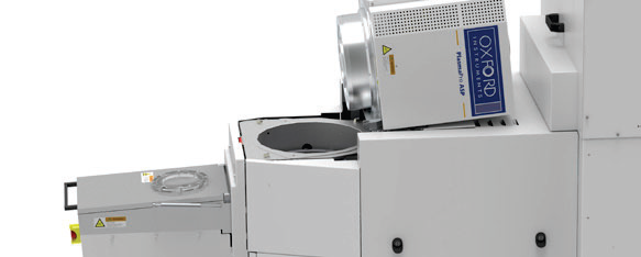
Image Credit: Oxford Instruments
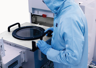
Image Credit: Oxford Instruments
Oxford Instruments Plasma Technology has developed a solution to this problem, specifically for engineers working with atomic layer deposition (ALD). The company offers a highly innovative and complementary pair of systems within its ALD product range that combine development flexibility with high-volume manufacturing repeatability and throughput.
Development with PlasmaPro ASP
The PlasmaPro ASP has been designed to offer process engineers the required capabilities and flexibility to develop the industry's most advanced and high-quality ALD layers suitable for research and development, while simultaneously ensuring incredibly high rates and low damage.
The PlasmaPro ASP was initially aimed at the quantum market when launched approximately two years ago. The instrument offers a deposition rate two-to-three times higher than that of comparable ALD systems, offering a robust process solution for superconducting nitrides, such as TiN and NbN.
The deposition of superconducting thin films can take up to 12–15 hours using rival tools, reducing implementation speed in some quantum applications.
Oxford Instruments identified an ideal set of processes to launch its PlasmaPro ASP, targeting the deposition of these superconducting nitrides. The company’s new ALD system offers deposition rates of over 25 nm per hour for NbN, and more than 35 nm per hour for TiN.
Alongside its capacity for rapid deposition rates, the PlasmaPro ASP can be used to tune film properties, such as crystallinity and stress, allowing engineers to achieve the exact desired properties for their deposited material.
Additional ALD films were developed after launching the PlasmaPro ASP with a suite of the most challenging thin films required for any application. These added capabilities provide Oxford Instruments’ customers with a genuinely distinct platform for ALD development.
Production with the Atomfab
The PlasmaPro ASP’s high deposition rates enable a key breakthrough for quantum applications, but these rates are not generally an essential requirement for ALD process development systems. Despite this, the PlasmaPro ASP has been designed to deliver these high rates to enable an innovative collaborative approach between the development and production of the company’s ALD systems and its Atomfab platform.
These platforms share the same design DNA, including an identical patented plasma source design and user interface, referred to as PTIQ.
This holistic product range concept allows the PlasmaPro ASP to offer a high deposition rate along with process flexibility and straightforward process transferability from development to the production-proven Atomfab ALD system.
Oxford Instruments has successfully shown that processes developed on its PlasmaPro ASP can be easily transferred to and replicated on the Atomfab. This characteristic is exceptionally beneficial to engineers who start by developing a process to deposit an ALD film, who can then rapidly ramp to production.
PlasmaPro ASP released. Source: Oxford Instruments
| Plasma ALD Material |
| NbN |
| TiN |
| Al2O3 (thermal) |
| TiO2 |
| AlN |
| HfO2 |
| Ga2O3* |
| GaN* |
* Data courtesy of TU/e.
Atomfab specification 200 mm. Source: Oxford Instruments
| Al2O3 |
AlN |
SiN |
| Within wafer thickness uniformity |
| < ± 1.0 % |
< ± 2.0 % |
< ± 3.0 % |
| Refractive index @ 632.8 nm |
| > 1.63 |
> 1.90 |
> 1.93 |
| Production stage |
| qualified |
validation |
validation |
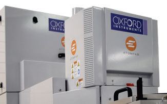
Image Credit: Oxford Instruments
The Atomfab has been production-qualified globally for ALD passivation of GaN HEMTs (high-electron-mobility transistors) since 2020.
The tool delivers a monthly throughput of more than 7000 wafers for oxide passivation, and over 9000 wafers for a nitride interface layer on GaN HEMTs for each ALD chamber on a cassette handler, when it has been optimized to run a single plasma ALD process on up to 200 mm wafers.
Throughput is vitally important for device fabrication, but quality is also essential. Oxford Instruments’ efforts in GaN HEMT device fabrication highlight this concept, with the company establishing a market-leading position in both ALD and atomic layer etch (ALE), while also demonstrating a range of processes designed to control and optimize material interfaces in order to improve device performance.
One such technique involves implementing a pre-ALD plasma surface treatment before performing nitride interfacial layer deposition. This combination optimizes the material interface, yielding excellent results.
These processes work in conjunction to reduce the interface trap density and improve the GaN HEMT device performance. This is achieved while also offering a considerably reduced cost of ownership (more than four times lower in cost versus the incumbent ALD solution) and meeting customers’ expectations in terms of the time to repair and clean, time between cleans, system uptime, and time between assists.
Accelerated development
The ability to perform high-rate ALD on a development system offers a diverse array of new opportunities for applying ALD where this has not previously been possible.
In addition to speeding up development, thicker ALD layers - that were previously not thought possible - can now be developed: it is now possible to consider ALD for new applications with a wider process application window.
Processes developed on the PlasmaPro ASP can be seamlessly transferred to Atomfab and ramped to production, allowing the use of ALD in high-volume device manufacturing.
Access to a suite of complementary products designed to achieve continuity between development and production phases offers major advantages, allowing developers to better keep pace with the fast-moving and innovative semiconductor device fabrication industry.
Acknowledgments
Produced from materials originally authored by Grant Baldwin and Dr. Aileen O'Mahony from Oxford Instruments Plasma Technology.
About Oxford Instruments
Oxford Instruments is a leading provider of high-technology tools and systems for research and industry, dedicated to accelerating breakthroughs that create a brighter future for our world. With a global presence, we are committed to innovation and excellence, offering cutting-edge solutions that enable researchers and industry professionals to achieve breakthroughs in their fields. Our advanced technologies deliver numerous benefits through unparalleled precision and reliability, allowing users to obtain accurate and reproducible results. By utilising Oxford Instruments' innovative solutions, research is accelerated, productivity is enhanced, and innovation is achieved in various fields, including materials analysis, life sciences, semiconductors, physics, chemistry, and food sciences. We take pride in being a trusted partner for those aiming to push the boundaries of scientific and industrial advancements, providing the tools and support necessary to realise their visions.
Atomic force microscopy: These advanced instruments are utilised for high-resolution imaging and precise measurement of surface properties at the nanoscale level. They offer detailed topographical information and enable accurate measurements of features such as height, roughness, and mechanical properties.
Light microscopy: Our solutions encompass a comprehensive range of advanced imaging systems that utilise visible light for examining samples at the microscale. Equipped with high-quality lenses, cameras, and illumination systems, these optical microscopes deliver detailed images with exceptional clarity and resolution. They find applications in fields such as biology, materials science, and forensics.
Plasma etch & deposition: innovative etch & deposition techniques, atomic layer etch and atomic layer deposition, and ionbeam etch & deposition solutions used to produce high yielding, efficient and reliable advanced semiconductor devices. Our service and product range includes research and development systems right through to fully clusterable, robust and high up-time production systems, designed for high-volume manufacturing in key markets like quantum, power devices, augmented reality and datacom.
Electron microscopy analysis: Our high-performance tools are tailored for materials characterisation, particle analysis, and sample manipulation at the nanometre scale. Techniques such as Backscatter Electron and X-ray (BEX), Energy Dispersive Spectroscopy (EDS), and Electron Backscatter Diffraction (EBSD) enable imaging, chemical analysis, and crystallographic characterisation of materials at atomic and nanoscale levels.
Optical imaging and spectroscopy: Our optical imaging solutions comprise a range of advanced technologies and systems for capturing and analysing images using light. From state-of-the-art optical microscopes to spectroscopy systems and imaging software, these solutions provide high-quality images and data for applications such as materials characterisation, biological research, and semiconductor analysis.
Nanoindentation: Our high-resolution, MEMS-based nanoindenters are designed to measure the mechanical properties of materials, including hardness, elastic modulus, stiffness, and creep behaviour. These instruments offer superior fabrication tolerances, enhancing sensitivity, resolution, and repeatability beyond conventional technology limits.
Nuclear Magnetic Resonance: We offer a variety of benchtop Nuclear Magnetic Resonance (NMR) instruments for research, industrial quality assurance/control, and rock core analysis. These instruments provide advanced capabilities for chemical analysis, materials characterisation, and more.
Raman microscopy: Our advanced imaging systems are tailored for high-resolution microscopy and analysis, offering cutting-edge technology and precision optics for detailed insights into samples at the micro- and nanoscales. Trusted by researchers and scientists in fields such as materials science, life sciences, and nanotechnology, these systems are available in various models to suit different applications.
X-ray technologies: Our technologies encompass a range of advanced systems and solutions for materials analysis and characterisation. With cutting-edge capabilities and high sensitivity, Oxford Instruments X-ray technologies are widely used in various industries and research academic institutions for applications such as material identification, quality control, and research in fields like geology, metallurgy, and semiconductor manufacturing.
Sponsored Content Policy: News-Medical.net publishes articles and related content that may be derived from sources where we have existing commercial relationships, provided such content adds value to the core editorial ethos of News-Medical.net, which is to educate and inform site visitors interested in medical research, science, medical devices and treatments.